[1] Photomasks are used at wavelengths of 365 nm, 248nm, and 193nm. Verifying and testing the dies on the wafer after the manufacturing. Verification methodology created from URM and AVM, Disabling datapath computation when not enabled. SRAM is a volatile memory that does not require refresh, Constraints on the input to guide random generation process. Fundamental tradeoffs made in semiconductor design for power, performance and area. The chrome materials arent etched in other places. This website uses cookies to improve your experience while you navigate through the website. Semiconductors that measure real-world conditions. A class of attacks on a device and its contents by analyzing information using different access methods. The difference between the intended and the printed features of an IC layout. Sensors are a bridge between the analog world we live in and the underlying communications infrastructure. Integrated circuits on a flexible substrate. Memory that stores information in the amorphous and crystalline phases. Finding out what went wrong in semiconductor design and manufacturing. Although they are designed to keep particles away, pellicles become a part of the imaging system and their optical properties need to be taken into account. C, C++ are sometimes used in design of integrated circuits because they offer higher abstraction. A data center facility owned by the company that offers cloud services through that data center. [4] In a fab, the mask as well as a wafer are inserted in a lithography scanner. Transformation of a design described in a high-level of abstraction to RTL. Features 150nm or below in size generally require phase-shifting to enhance the image quality to acceptable values. Testbench component that verifies results. Making a mask of this sort became increasingly difficult as the complexity of the designs increased. The absorber is a 3D-like feature that juts out on top of the mask. A way to improve wafer printability by modifying mask patterns. This was the standard for the 1:1 mask aligners that were succeeded by steppers and scanners with reduction optics. The commonly used attenuated phase-shifting mask is more sensitive to the higher incidence angles applied in "hyper-NA" lithography, due to the longer optical path through the patterned film. [1] As feature sizes shrank and wafer sizes grew, multiple copies of the design would be patterned onto the mask, allowing a single print run to produce many ICs. When channel lengths are the same order of magnitude as depletion-layer widths of the source and drain, they cause a number of issues that affect design. Electronic Design Automation (EDA) is the industry that commercializes the tools, methodologies and flows associated with the fabrication of electronic systems. (Imec, KU Leuven, Ghent University, PTB). Method to ascertain the validity of one or more claims of a patent. Crypto processors are specialized processors that execute cryptographic algorithms within hardware.
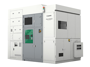
fpa stepper canon semiconductor lithography equipment global semicon indtech IEEE 802.11 working group manages the standards for wireless local area networks (LANs). It has been used in a number of instruments to split a beam of light without causing an optical path shift due to its small film thickness. Beginning in the 1960s, thin film stretched on a metal frame, also known as a "pellicle", was used as a beam splitter for optical instruments. This issue, known as mask 3D effects, can result in unwanted pattern placement shifts. A method for growing or depositing mono crystalline films on a substrate. A neural network framework that can generate new data. Finally, a pellicle, a thin membrane, is mounted on top of the mask, which protects the mask from falling particles or contamination. Generally, a photomask consists of templates of several dies of a given IC design. As leading-edge semiconductor features shrink, photomask features that are 4 larger must inevitably shrink as well. A transistor type with integrated nFET and pFET. A software tool used in software programming that abstracts all the programming steps into a user interface for the developer. It is mandatory to procure user consent prior to running these cookies on your website. In operation, light hits the mask and goes through the areas with the glass, which exposes the wafer. Light used to transfer a pattern from a photomask onto a substrate. A measurement of the amount of time processor core(s) are actively in use. Measuring the distance to an object with pulsed lasers. Memory that loses storage abilities when power is removed. This was solved with the introduction of the optical pattern generator which automated the process of producing the initial large-scale pattern, and the step-and-repeat cameras that automated the copying of the pattern into a multiple-IC mask. A different way of processing data using qubits. The energy efficiency of computers doubles roughly every 18 months. Complementary FET, a new type of vertical transistor. An IC created and optimized for a market and sold to multiple companies. A 2005 study by IMEC found that thinner absorbers degrade image contrast and therefore contribute to line-edge roughness, using state-of-the-art photolithography tools. What are the types of integrated circuits? A power semiconductor used to control and convert electric power. Special purpose hardware used for logic verification. The integrated circuit that first put a central processing unit on one chip of silicon. Power creates heat and heat affects power. Reuse methodology based on the e language. Making masks At a photomask manufacturer, the materials on the blank are patterned using an e-beam mask writer.
lithography hynix sk wafer nanoimprint semiconductor develop kitguru memory This all depends on the device type. The mask is then inspected for defects. IEEE 802.1 is the standard and working group for higher layer LAN protocols. (However, some photolithography fabrications utilize reticles with more than one layer patterned onto the same mask). A type of field-effect transistor that uses wider and thicker wires than a lateral nanowire. The variation of electron beam scattering in directly writing the photomask pattern can easily well exceed this.[13][14]. Colored and colorless flows for double patterning, Single transistor memory that requires refresh, Dynamically adjusting voltage and frequency for power reduction. The basic architecture for most computing today, based on the principle that data needs to move back and forth between a processor and memory. Verification methodology built by Synopsys.

Adding extra circuits or software into a design to ensure that if one part doesn't work the entire system doesn't fail. Google-designed ASIC processing unit for machine learning that works with TensorFlow ecosystem. Lithography using a single beam e-beam tool. Code that looks for violations of a property. Commonly and not-so-commonly used acronyms. A set of unique features that can be built into a chip but not cloned.

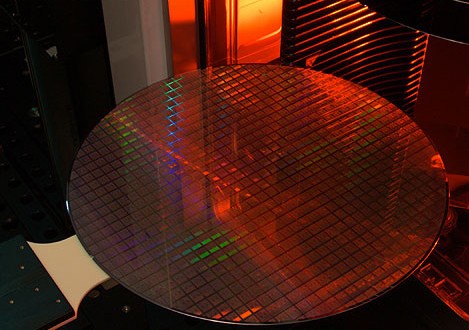
In the semiconductor process flow, a chipmaker first designs an IC, which is then translated into a file format. A photomask is protected from particles by a pellicle a thin transparent film stretched over a frame that is glued over one side of the photomask. Data can be consolidated and processed on mass in the Cloud.
oled mask production fmm samsung amoled smd shadow info developed makers offering early start manufacturing stronger masks [3] To achieve complete wafer coverage, the wafer is repeatedly "stepped" from position to position under the optical column until full exposure is achieved. Integrated circuit layout design protection, Lithography experts back higher magnification in photomasks to ease challenges, "ULTRA Semiconductor Laser Mask Writer | Heidelberg Instruments", "Large Area Photomask Writer VPG+ | Heidelberg Instruments", "Photomasks - Photolithography - Semiconductor Technology from A to Z - Halbleiter.org", "Toppan Photomasks Inc. - Photomasks - The World's Premier Photomask Company", "Semiconductor Photomask Market: Forecast $3.5 Billion in 2014", "SEMI Reports 2013 Semiconductor Photomask Sales of $3.1 Billion", An Analysis of the Economics of Photomask Manufacturing Part 1: The Economic Environment, "Mask Cost and Profitability in Photomask Manufacturing: An Empirical Analysis", https://en.wikipedia.org/w/index.php?title=Photomask&oldid=1092078708, Articles with unsourced statements from May 2022, Creative Commons Attribution-ShareAlike License 3.0, This page was last edited on 8 June 2022, at 02:21. Locating design rules using pattern matching techniques. A digital signal processor is a processor optimized to process signals. A possible replacement transistor design for finFETs. Coverage metric used to indicate progress in verifying functionality. (Levenson has since retired.). Almost half of the market was from captive mask shops (in-house mask shops of major chipmakers). Next-generation wireless technology with higher data transfer rates, low latency, and able to support more devices. Source: Wikipedia. [6], Photomasks are made by applying photoresist to a quartz substrate with chrome plating on one side and exposing it using a laser or an electron beam in a process called maskless lithography. A technical standard for electrical characteristics of a low-power differential, serial communication protocol. Using a tester to test multiple dies at the same time. A basic blank consists of a quartz or glass substrate, which is coated with an opaque film. In these systems there may be no reticle, the masks can be generated directly from the original computerized design. Copper metal interconnects that electrically connect one part of a package to another. The integration of photonic devices into silicon, A simulator exercises of model of hardware. Deviation of a feature edge from ideal shape. In optical lithography, a mask consists of an opaque layer of chrome on a glass substrate. The mask with the pellicle on top is then shipped to the fab. A secure method of transmitting data wirelessly. Attenuated phase-shift masks also resemble a binary mask. Special flop or latch used to retain the state of the cell when its main power supply is shut off. For this, a photomask maker etches the chrome in select places, which exposes the glass substrate. Completion metrics for functional verification. A dense, stacked version of memory with high-speed interfaces that can be used in advanced packaging. Interconnect standard which provides cache coherency for accelerators and memory expansion peripheral devices connecting to processors. An approach to software development focusing on continual delivery and flexibility to changing requirements, How Agile applies to the development of hardware systems. Sci. A lab that wrks with R&D organizations and fabs involved in the early analytical work for next-generation devices, packages and materials. To mask a photomask, the first step is to create a substrate or mask blank. A semiconductor company that designs, manufactures, and sells integrated circuits (ICs). The emergence of immersion lithography has a strong impact on photomask requirements. Cobalt is a ferromagnetic metal key to lithium-ion batteries. There are two types of phase-shift masks, alternating and attenuated. This site uses cookies. An artificial neural network that finds patterns in data using other data stored in memory. This helped drive the adoption of reticles, which were used to produce thousands of masks. [15], The SPIE Annual Conference, Photomask Technology reports the SEMATECH Mask Industry Assessment which includes current industry analysis and the results of their annual photomask manufacturers survey. Application specific integrated circuit (ASIC), Application-Specific Standard Product (ASSP), Atomic Force Microscopy (AFM), Atomic Force Microscope (AFM), Automotive Ethernet, Time Sensitive Networking (TSN), Cache Coherent Interconnect for Accelerators (CCIX), CD-SEM: Critical-Dimension Scanning Electron Microscope, Dynamic Voltage and Frequency Scaling (DVFS), Erasable Programmable Read Only Memory (EPROM), Fully Depleted Silicon On Insulator (FD-SOI), Gage R&R, Gage Repeatability And Reproducibility, HSA Platform System Architecture Specification, HSA Runtime Programmers Reference Manual, IEEE 1076.4-VHDL Synthesis Package Floating Point, IEEE 1532- in-system programmability (ISP), IEEE 1647-Functional Verification Language e, IEEE 1687-IEEE Standard for Access and Control of Instrumentation Embedded, IEEE 1801-Design/Verification of Low-Power, Energy-Aware UPF, IEEE 1838: Test Access Architecture for 3D Stacked IC, IEEE 1850-Property Specification Language (PSL), IEEE 802.15-Wireless Specialty Networks (WSN), IEEE 802.22-Wireless Regional Area Networks, IEEE P2415: Unified HW Abstraction & Layer for Energy Proportional Electronic Systems, Insulated-Gate Bipolar Transistors (IGBT), ISO/SAE FDIS 21434-Road Vehicles Cybersecurity Engineering, LVDS (low-voltage differential signaling), Metal Organic Chemical Vapor Deposition (MOCVD), Microprocessor, Microprocessor Unit (MPU), Negative Bias Temperature Instability (NBTI), Open Systems Interconnection model (OSI model), Outsourced Semiconductor Assembly and Test (OSAT), Radio Frequency Silicon On Insulator (RF-SOI), Rapid Thermal Anneal (RTA), Rapid Thermal Processing (RTP), Software/Hardware Interface for Multicore/Manycore (SHIM) processors, UL 4600 Standard for Safety for the Evaluation of Autonomous Products, Unified Coverage Interoperability Standard (Verification), Unified HW Abstraction & Layer for Energy Proportional Electronic Systems, Voice control, speech recognition, voice-user interface (VUI), Wide I/O: memory interface standard for 3D IC, Anacad Electrical Engineering Software GmbH, Arteris FlexNoC and FlexLLI product lines, Conversant Intellectual Property Management, Gradient DAs electrothermal analysis technology, Heterogeneous System Architecture (HSA) Foundation.
Sitemap 19